Bosch K-jet Lambda Controllers
0280 800 001 and 0280
800 021 Notes on Operation

Purpose of Unit
These controllers vary the mixture of fuel and air by controlling the fuel flow through an electrically operated fuel valve (called a lambda valve or frequency valve) which in turn controls the pressure under a mechanical fuel distributor’s diaphragms to affect the rate of fuel flow for a given air flow. The unit uses input from a zirconia oxygen sensor (lambda sond), and a thermal switch during warmup.
Power Distribution
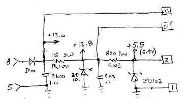
Power for the internal circuits enters on pin 8. D100 provides reverse polarity protection; C100 decouples any higher frequency noise on the supply line. After R100, ZD101 appears to be in place for overvoltage protection, as it does not limit at up to 14.0V in. Further decoupling is provided by C105, after which R103 and ZD102 form a 5.9V stable source.
Grounds are separated by function for small signal circuitry and output drivers. The high current output circuits are grounded through pin 16; the remaining circuitry grounds at pin 5 and shield for the lambda sensor cable is grounded at pin 4.
Lambda Sond Input
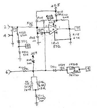
The input circuitry consists of half of a 532 op amp, IC1a, and associated components.
The sensor voltage arrives at pin 2. IC-1a is configured as a high gain inverting amplifier to result in a comparator function. The reference for comparison is the voltage at pin 3 established for the main part by a voltage divider composed of R104, 105, 106, 112 and 108 from the stable +5.5V. The resulting reference is 0.50V normally, but under certain conditions is modified by voltage applied through D510 or external pin 6.
With the amplifier IC-1a pin 3 reference set at 0.50 volts, any voltage in excess of 0.50 developed by the lambda sond through external pin 2 results in IC-1a output being driven to the lower rail at 0.6V. As the input decreases, crossing 0.50V, the comparator output is driven to the upper rail at 11.4V.
External pin 6 can influence the reference voltage. For instance, if pin 6 is grounded, the comparator switches at a very lean 0.15V. The application for the -001 control unit is supposed to be a 1977-79 Volvo B21f and for the -021, a 1980 B21f, and none of these models have any connection to pin 6 in their harness wiring diagrams. Instead of being used as an input, perhaps pin 6 is a test point to monitor comparator reference point with a meter.
Through D510, the reference voltage is increased beginning about 5 seconds after the comparator has continuously sensed a rich mixture, or higher than 0.50V at the lambda sond input. This voltage is developed by the timer and ramp-up circuitry of T500, T501, C500 and associated components. As the reference increases, so does the lambda sond input voltage necessary to keep the comparator output at low rail. Any subsequent reduction at the input reverses the direction of the timer’s reference voltage bias and allows the voltage passed by D510 to be ramped down again.
If there is no input at external pin 2, such as when the lambda sond is disconnected or too cold to flow current, the internal offset or leakage current within IC-1a will charge C103 to about half supply, or 6.5V. This current is very small, such that even a 10M-ohm input meter will quickly discharge C103 to below comparator reference, but if left open will keep IC-1a’s output pin held low.
If the input voltage remains higher than the reference, after about 12 seconds timer circuit IC-2a, T502, pulls to ground allowing the T500/T501 timer to immediately rise to 5.5V. T502 also immediately cuts off T501 through D506 and T500, forward biasing D511 and D512. This results in a small current to the lambda sond input pin that will allow it to remain at least 2.5V until the lambda sond is warm enough to produce its own current, swamping the weaker current through R523.
Summarizing the input comparator and influences, the normal operation comparator crossover point is 0.5V. It is modified upward (richer) to about 1.2V according to the amount of time continuously spent above this value in excess of about 5 seconds. If the input remains higher than this increased reference after 12 seconds, the lambda sond input is deemed open (or cold) and this information is used to normalize the fuel adjustment in subsequent circuits until the sensor input returns to its expected 0.1-0.9V range.
Signal Conditioner/Inverter
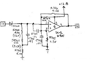
IC-2b, C700 condition the on/off output of the input comparator. When the sensor’s voltage is below reference, the comparator output is high and D700 is forward biased quickly charging C700 to about 10.9V. IC-2 is a quad comparator with open collector output (2901). IC-2b has a fixed reference on the non-inverting pin set at 3.2V, so the 10.9 on the inverting pin (4) results in the output being pulled to ground.
When the sensor’s voltage indicates richer than stoichiometric, climbing above 0.5V, D700 is no longer forward biased, so C700 discharges through R700/R701 and the output pin 2 switches to 9.0V as the voltage on C700 decreases through the reference 3.2V level.
Open-loop Timer
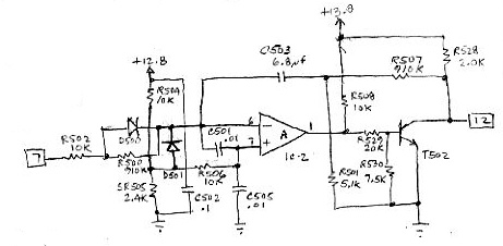
IC-2a, C503, and T502 form a 12-second timer circuit started when IC-1a’s output first goes low. As C503 charges through R502, D500 higher than the 2.5V established at reference pin 7, IC-2a pin 1 pulls to ground. T502 inverts this, remaining cutoff until the input mixture is sensed rich, reverse biasing D500, when C503 again discharges through R500 in about 12 seconds to less than 2.5V. At the end of the 12 seconds T502 saturates, indicating a probable cold or missing lambda sond.
This open-loop indication is used several ways.
- Through forward bias of D514, it halts the operation of the ramp generator used to adjust the duty cycle of the lambda valve.
- Through D513, it sets that duty cycle to a predetermined midrange value.
- Buffer and driver T400 and T401 provide an external open-collector output at pin 14.
- Through D506 and D505, the input comparator reference adjustment is set at maximum.
Closed Loop Compensator
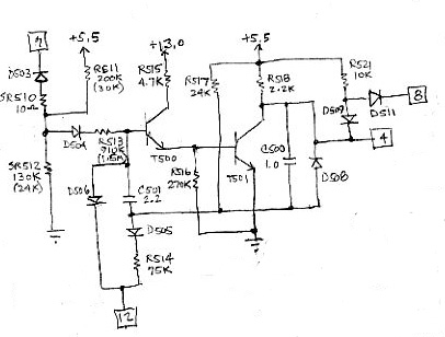
C500, C501, T500, and T501 define the operation of a timer that ramps up the input comparator’s reference signal according to the amount of time elapsed since the last lean crossing, or high rail output from the comparator IC-1a. Once IC-1a output goes low, D503 becomes forward biased, removing the forward bias from D504. C501 begins to discharge slowly through T500’s base-emitter junction, easing T501 out of saturation.
Once the voltage at the collector of T501 reaches 900 mV, D510 begins to conduct, adding to the comparator reference. The action of T500 and T501 is to slowly ramp this reference up until it is matched by the lambda sond input, when IC-1a’s output will switch high, resulting in the reversal of the ramp when D504 again becomes forward biased. The timing of ramp down is faster, resulting in rapid switching at the comparator’s output as the reference voltage tracks a slowly changing input signal.
If this reversal does not happen within the 12 second period allowed by the Open Loop Timer, D506 and D505 conduct to immediately discharge the Closed Loop timer. Any input voltage greater than 1.2V, the limit of reference compensation, will latch T501’s collector to 5.5V, placing the comparator in open loop mode, forward biasing D511 and D512 to provide 2.5V through R523 to the lambda sond input pin.
Ramp Generator
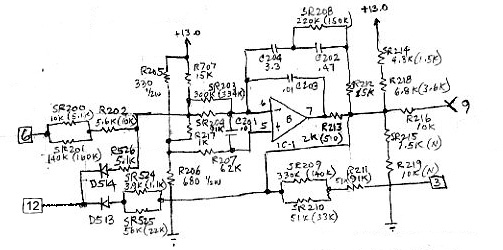
IC-1b, C204, C202, and a host of precision selected resistors comprise a 10-second ramp generator that is used to set the duty cycle of the lambda valve in either a leaning or a richening effect based on its input from the lambda sond. Its main input is a binary signal from the Signal Conditioner/Inverter which is 0V when opening up the lambda valve (calling for rich mixture) and 9V when shutting it down to lean out the mixture. Its main output is the input to the Pulse Width Modulator that forms the signal that eventually drives the lambda (frequency) valve.
The ramp’s time constant forces the mixture adjustments to be somewhat gradual, not abrupt, allowing for the delay in the engine’s performance and closed loop detection of it by the lambda sond.
IC-1b is configured to operate as a precision amplifier whose non-inverting input (5) is fixed at 8.8V by divider pair R205/R206 through R207. DC operating point on the inverting input (6) is initially set slightly positive from the 8.8V reference with a further divider pair, R207/R217. Output (7) varies as the charging of C204/C202 increasing to full charge at 11.5V if IC-2c’s output remains at 0V (calling for more fuel). When the lambda sond detects this extra fuel, IC-2c’s output rises to 9V, through R200, R201, R202, and R207.
This begins the discharge of the capacitors and the timed fall of IC-1b’s output voltage until either it reaches its low rail at 0.7V or its direction is again reversed by the comparator’s output.
A secondary input to the Ramp Generator disables it when the Open Loop Timer times out. D514 is forward biased, dropping the pin 6 voltage to latch the output to the upper rail. D513 is also biased on to divide the output voltage of IC-1b giving a fixed mid-range value near 7.7V during open loop conditions.
Pulse Width Modulator
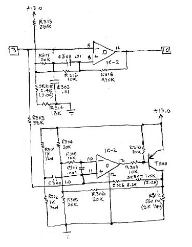
IC-2d, IC-2c and T300 make up a circuit that generates a rectangular waveform whose duty cycle is inversely proportional to the DC input voltage supplied by the Ramp Generator. IC-2c and T300 form a fixed feedback oscillator supplying a fixed-frequency (66Hz) triangle wave voltage added to the Ramp Generator output at IC-2d’s inverting input (8). IC-2d is configured as a comparator with fixed reference at 6.9V on its + input (9). R318 adds some hysteresis in the form of positive feedback to keep the output non-linear.
In the oscillator section, C300 is charged and discharged through R326/R307 as T300 switches on and off. IC-2c compares the state of C300’s charge to the voltage on IC-2c’s inverting pin (10) which changes from 1/3 to 2/3 supply based on the divider R303/R305 and feedback through R307 from T300 collector. This results in a symmetrical triangular waveform on C300 varying between 4 and 8 volts.
As the output of the Ramp Generator is summed with the triangular waveform from IC-2c pin 11, IC-2d’s pin 14 snaps low when the tips of the triangle waveform added to the ramp output surpass the reference 6.9V. As the ramp output increases, so does the time pin 14 is pulled low, compared with the remaining time. At maximum output from the ramp generator, the time pin 14 is pulled low is near 86%; at minimum it is 5%.
External driver circuits
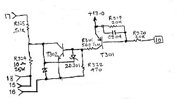
T301 and T302 form the driver for the lambda valve. The output of the Pulse Width Modulator is inverted by T301 and again by T302, the power driver for the valve. A separate high-current ground reference is used to sink the valve current at external pin 16. The valve is connected between battery (supplied through an external relay) and pin 15 of the lambda controller. Power resistor, R324 limits the valve current, while D300 and ZD301 protect the transistor from coil collapse voltages. A test point, for measuring duty cycle, is provided at external pin 17.
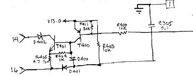
T400 and T401 provide a similar function to buffer and drive an output of the Open Loop Timer. T401 provides an open collector output when the controller detects the open loop condition. This function does not appear to be used in the Volvo, but using the size of the power transistor and its heat sink as a guide, the circuit appears to have been designed to drive a relay or perhaps a fault indicator lamp.